Matthias Köfferlein
Matthias Köfferlein
Please refer to this discussion for details: https://www.klayout.de/forum/discussion/1699/layoutview-on-selection-changed-behavior#latest

With the new "universal DRC" functions, it's possible to code a DRC check like this: ``` m1 = input(16, 0) m1.drc(width >= 1.15).output(100, 0) ``` The behavior of "width >...
For details see this discussion: https://www.klayout.de/forum/discussion/1733/changing-layoutview-title#latest
See https://www.klayout.de/forum/discussion/1601/array-instance-counts-identified-by-detailed-layer-statistics#latest for details.
Apparently (user report) with a M specification, the total width of a transistor needs to be computed by multiplying with M. KLayout internally uses the full width, not the width...
To reproduce do this: * create/load a larger, hierarchical netlist, preferably with many small circuits into the netlist browser * In the right-side tree, expand all nodes (context menu) *...
The attached GDS file produces an artefact sliver on this (extreme) undersize: ``` input(36, 0).sized(-127.um).output(1000, 0) ``` [m5.gds.zip](https://github.com/KLayout/klayout/files/3694842/m5.gds.zip) 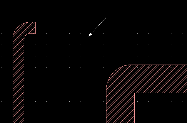
See https://www.klayout.de/forum/discussion/1337/trace-net-observation#latest for details.
For the story see: https://www.klayout.de/forum/discussion/1220/save-visible-layers-with-pcells
See https://www.klayout.de/forum/discussion/1065/tech-file-enhancement-proposal-net-name#latest