CPU bus functional test
This test should verify that the CPU performs the correct read's and write's on the external bus. This is important when addressing I/O devices, and this issue is created as a result of this comment: https://github.com/sy2002/QNICE-FPGA/issues/9#issuecomment-670980704.
This issue is non-trivial to implement, and is therefore separate from the existing CPU test suite discussed in Issue #9.
Below are the ideas I have so far. I welcome any feedback, improvements, critique, etc. I propose this issue be targeted for release V1.7, simply because we already have a lot of stuff in V1.6.
Proposed solution
A new I/O device will be developed (in both hardware and the emulator) with the following register map:
0xFF80 : Regular R/W scratch register
0xFF81 : Regular R/W scratch register
0xFF82 : Unused (?)
0xFF83 : Unused (?)
0xFF84 : Counts number of reads from 0xFF80. Writeable
0xFF85 : Counts number of reads from 0xFF81. Writeable
0xFF86 : Counts number of writes to 0xFF80. Writeable
0xFF87 : Counts number of writes to 0xFF81. Writeable
Proposed use case
The test code will look something like:
MOVE 0xFF81, R1
CMP 0, @--R1
The above code is expected to perform 1 read from 0xFF80, and no writes. So the test will clear all counters, then perform the above two instructions, and then verify the four counters have the correct values.
The test will then repeat with all instructions and all pairs of addressing modes.
One more thing. On the hardware, this test should also verify that the signal WAIT_FOR_DATA doesn't create spurious accesses, i.e. that the read and write counts are unaffected.
Are there any of the existing I/O devices that use this signal ?
@MJoergen Some background about WAIT_FOR_DATA: It is an input signal of the CPU (code link) which is adding wait-states when devices need longer than 1/2 of a cycle to deliver or to store data.
The standard timing is: The CPU puts an address to the address bus at the rising edge of the CPU internal execution step n and expects the data to be there (for reading) at the rising edge of the next cycle n+1 or written at the end of the next cycle n+1. (BTW off-topic, because not related to WAIT_FOR_DATA: When it comes to working with the registers the timing is a bit tougher: The address, which register is to be read or written is being put on the internal register bus at the rising edge and the values are expected to be there at the falling edge: This gives the register memory a bit time to settle and deliver but we are not wasting a full cycle. This is also why in the register handling part of the devices you should see if falling_edge(clk) then statements.)
If a device is not able to deliver (or to digest the data) that quickly, then it pulls up WAIT_FOR_DATA from 0 (which means "do not add wait-cycles") to 1 (which means "do add wait-cycles"). WAIT_FOR_DATA is currently implemented at the following execution stages of the CPU:
cs_fetch: For being able to wait for slow RAM to deliver the next operationcs_exeprep_get_src_indirect: For being able to wait for slow RAM or any other device to deliver the value of an indirectly adressed source valuecs_exeprep_get_dst_indirect: Ditto, but for the destination valuecs_exepost_store_dst_indirect: For being able to wait for slow RAM or any other device to store the destinaton value
In mmio_mux there is an output signal cpu_wait_for_data to the CPU (code link). Now, this was quite a bit of preface to the simple question if there would be any devices that are using this signal 😄 You find the list of them in mmio_mux in the process cpu_wait_control (code link). Without further ado, here is the answer to your original question:
- RAM
- ROM
- PORE ROM
- UART
(Note to self: We might want to start a doc/architecture.md or something where all this kind of info is collected. Will make a new issue for 1.7 or later and assign it to you and me).
I've started development on this on the separate branch dev-cpu-bus-test.
It works in the simulator, but something fails in the hardware. I have not debugged that yet.
The CPU Bus Test requires a new I/O module (currently placed at 0xFF80) in both the hardware and the emulator. In the emulator I have introduced the conditional compile flag USE_CPU_BUS_TEST. There is currently no similar compile flag for the FPGA.
We need to discuss whether to leave this module in the FPGA and/or emulator permanently, or whether we should just have it in temporarily until we're satisfied the CPU works as expected.
We need to discuss whether to leave this module in the FPGA and/or emulator permanently, or whether we should just have it in temporarily until we're satisfied the CPU works as expected.
- I suggest to leave it always in the FPGA, as long as we are not running out of MMIO space, because as far as I understand, this will not have any negative impact on the system.
- Furtheron I suggest to put it in the "upper" area of our MMIO, i.e. 8 words below where the MEGA65 starts, which would be
FFE8, if I calculated correctly. - When it comes to the emulator, it is our best practice, that in principle, all MMIO devices can be switched ON/OFF via defines. Just like you did it already in the branch, as far I as saw it. And yes, I would also suggest to leave it always on, in the emulator, too, i.e. the make bash files of the UART emulator, the VGA emulator and the WASM emulator need to be adjusted accordingly
Not sure if this is a bug or not.
I've started debugging the CPU Bus Test (CBT) on the hardware, and it fails on the first instruction: CMP R0, @R2.
The attached picture shows what is happening:
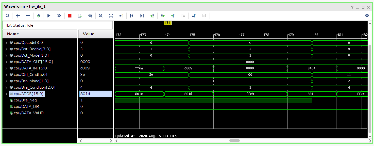
The CPU fetches the instruction (0xC009, which is CMP R0, @R2) from address 0x801D, and then performs a single read from address 0xFFE9 (which is the contents of register R2). However, the read lasts for three clock cycles, and therefore the CBT block counts this as reading three times.
Ideally, I would like a "Read Enable" signal from the CPU to indicate when a read is taking place. This signal would only be asserted for one clock cycle (of the three clock cycles the instruction takes).
The alternative is to change the CBT module so that it "recognizes" that the three consecutive clock cycles should all count as one read. I'm hesitant with this solution, because the idea of the CBT module is precisely to catch the errors where the CPU performs additional (unexpected) reads/writes.
A second alternative is to change the cpu_bus_test.asm code so that it does not check for equality with the expected value, but only check for zero/nonzero.
What are your thoughts on this @sy2002 , @bernd-ulmann ?
Here's another screen shot with a different instruction:
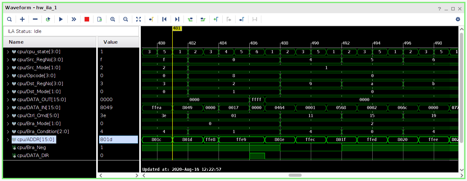
This shows the execution of the instruction NOT @R0, @R2 (0x8049), where R0 = 0xFFE8 and R2 = 0xFFE9.
We see that the CPU performs a single read from 0xFFE8, and then spends three clock cycles accessing 0xFFE9, where the first two cycles are read, and the last cycle is a write. I would expect a single clock cycle to read from 0xFFE8 and a single clock cycle to write to 0xFFE9. The two cycles reading from 0xFFE9 are wrong in my opinion.
Right now, I would say this is "works as designed" - but it is not well designed by me :-)
This is due to the wait state handling of the RAM (please see the comment above about WAIT_FOR_DATA) and the very cautious way the CPU handles it. The motto is "it is better to loose one cycle than to have corrupt data". BUT: Obviously - and I do acknowledge that - I were way to conservative in many places.
So this is for sure something that I would love to handle in V1.7 (but not in V1.6 any more): Please either spawn a new issue and assign it to me with this very topic inside it (maybe having some links to your comment of this issue - or copy some content) or rename this issue, assign it to me and make a new one for handling your CPU bus functional test.
Here some more color:
CMP R0, @R2 runs through these stages:
cs_fetch
cs_decode
cs_exeprep_get_dst_indirect (**)
cs_execute
At the point of (**) there is this code
         when cs_exeprep_get_dst_indirect =>
            -- add wait cycles, if necessary (e.g. due to slow RAM)
            if WAIT_FOR_DATA = '1' then
               fsmNextCpuState <= cs_exeprep_get_dst_indirect;

            -- data from bus is available
            else
               -- read the indirect value from the bus and store it
               fsmDst_Value <= DATA_IN;
            end if;
You see: It is adding wait states due to the RAM telling it that it should. So the behaviour of the MMIO devices (here: the RAM) needs to be optimized and here and there the CPU state machine needs to be tuned/tweaked/optimized.
NOT @R0, @R2 runs through these stages
cs_fetch
cs_decode
cs_exeprep_get_src_indirect
cs_exeprep_get_dst_indirect
cs_execute
cs_exepost_store_dst_indirect
Conclusion
So for now, I would suggest, that your cpu_bus_test.asm recognizes this behaviour - for V1.6 as "acceptable because works as designed" - and then in V1.7 we tackle this together with all the other "not-so-clean" stuff in QNICE-FPGA such as issue #57 .
I don't want to divert this discussion too much, but I have two comments:
- You mention
WAIT_FOR_DATA. With the changes to the tristate handling, the RAM no longer assertsbusy, and therefore theWAIT_FOR_DATAdoesn't get asserted either. I'll include this signal in the ILA next time, just to be sure. - You mention four CPU states for the instruction
CMP R0, @R2, but the ILA trace above shows five clock cycles. The screen shot doesn't show the CPU state, so I'll check that in ILA next time as well.
Getting back to your comment, we can safely defer any changes to V1.7. In fact, this issue is already tagged V1.7 ! I guess I'll just leave the current implementation in the branch dev-cpu-bus-test, and just not merge it into the develop branch until we've safely released V1.6.
OK thank you - let's proceed like that.
And we might want to use our upcoming Thursday ILA session to have a look at this very case together ;-)
My take on your second point would be, that the CPU stretches one of the four states to be two cycles long due to a wait state summing up to five cycles.