netlistsvg
 netlistsvg copied to clipboard
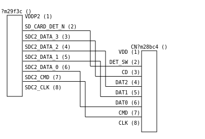
Nets that should stay parallel get tangled up
I wanted to draw a page of a bigger schematic that would focus only on the SD card interface.
Something like this:

Usually you have a very small subset of the SOC on one side, the sd card connector on the other side. You might see pull up resistors, some inline resistors.
Netlistsvg wasn't very happy though. Even without any resistors.
source.json
{
	"modules": {
		"SVG Output": {
			"cells": {
				"U?m29f3c()": {
					"connections": {
						"VDDP2 (1)": [
							0
						],
						"SD_CARD_DET_N (2)": [
							1
						],
						"SDC2_DATA_3 (3)": [
							2
						],
						"SDC2_DATA_2 (4)": [
							3
						],
						"SDC2_DATA_1 (5)": [
							4
						],
						"SDC2_DATA_0 (6)": [
							5
						],
						"SDC2_CMD (7)": [
							6
						],
						"SDC2_CLK (8)": [
							7
						]
					},
					"port_directions": {
						"VDDP2 (1)": "output",
						"SD_CARD_DET_N (2)": "output",
						"SDC2_DATA_3 (3)": "output",
						"SDC2_DATA_2 (4)": "output",
						"SDC2_DATA_1 (5)": "output",
						"SDC2_DATA_0 (6)": "output",
						"SDC2_CMD (7)": "output",
						"SDC2_CLK (8)": "output"
					},
					"type": "U?m29f3c ()"
				},
				"CN?m28bc4()": {
					"connections": {
						"VDD (1)": [
							8
						],
						"DET_SW (2)": [
							1
						],
						"CD (3)": [
							2
						],
						"DAT2 (4)": [
							3
						],
						"DAT1 (5)": [
							4
						],
						"DAT0 (6)": [
							5
						],
						"CMD (7)": [
							6
						],
						"CLK (8)": [
							9
						]
					},
					"port_directions": {
						"VDD (1)": "input",
						"DET_SW (2)": "input",
						"CD (3)": "input",
						"DAT2 (4)": "input",
						"DAT1 (5)": "input",
						"DAT0 (6)": "input",
						"CMD (7)": "input",
						"CLK (8)": "input"
					},
					"type": "CN?m28bc4 ()"
				}
			},
			"ports": {}
		}
	}
}
Note that the nets are actually in the proper order, it's not like they're swapped. Swapping the cell order does make a little bit of a difference, but there's still tangled up nets.
Yeah, thia is sort of fundamental to how the layout engine works. Layered graph layout techniques are not very successful when there is two directions of flow. Digital schematics do well because all of the signals go left to right but analog schematics have horizontal and vertical elements. Right now the analog skin is optimized for vertical layouts which makes things like VCC and GND and vertical components look clean and not have any unnecessary bends but horizontal paths like yours always look terrible. Without your resistors a horizontal flow would probably do an okay job. But the vertical resistors probably would not look very nice. A horizontal flow would probably pile up the resistors above or below the generic component on the right.
I think the only way to really fix this issue is to avoid using ELK altogether and write a layout algorithm that would correctly place the resistors vertically above the generic components and place the resistors horizontally between the generic components.
That wouldnt be like a weekend project though so I wont have anything like that soon.
You could also raise on issue on the ELK repo about this though and they could take a look at it. I'm just not optimistic.
I tested your JSON again with newer versions of ELKjs and it seems like it comes out closer to what you were wanting.
