netlistsvg
 netlistsvg copied to clipboard
annotate ports traces and junctions with a net id
This would simplify mapping the schematic parts to the pcb.
Annotating component id's would also be useful
Yes please! I want this a lot for my uses.
A way for a label to show up on a net. I don't think there's even a way to provide net name right now in the schema, just node number.
Once that's done. It would be nice to show nets that only connect to one place but is labeled/named.
This way you could do airwires:
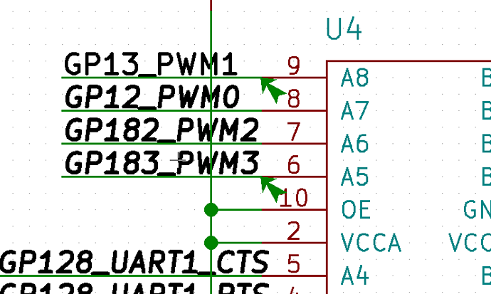
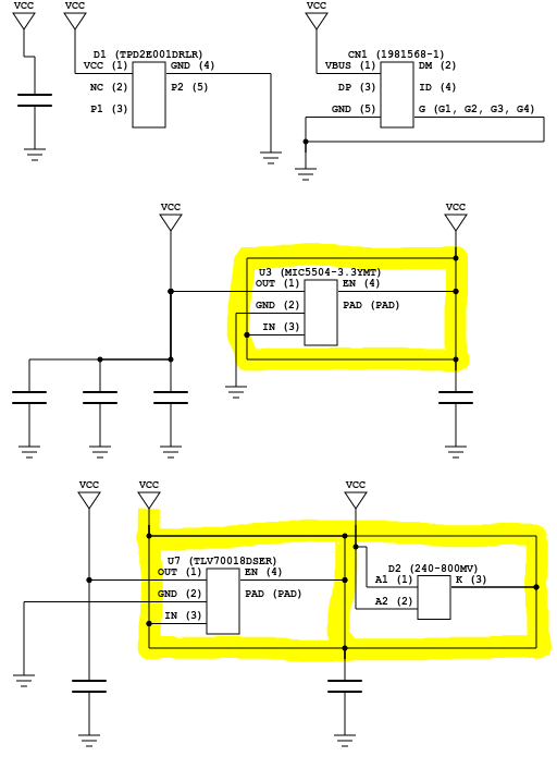
Right now I have to either use ports, or just live with the fact that my pin that only connects to one net node doesn't show anything connected to it (see CN1.{DP, DM}):
This is actually very doable because yosys netlists contain net names and ELK supports edge labels. So should be pretty straightforward.
Cool. I saw hints in the schema about this.
So I guess we'll be able to do:
"netnames": {
	"PP3300": { "bits": [ 1 ] }
	"GND": { "bits": [ 2 ] }
	"VBUS": { "bits": [ 3 ] }
	....
}
The name bits is not very semantic for analog, but I assume it's something dictated by yosys.
How would the output of elkjs be processed to keep the net names nearby? I guess a
PS: Why does the schema also talk about "0" and "1" instead of the node numbers? What does that allow us to do?
How would the output of elkjs be processed to keep the net names nearby?
ElkModel.wireNameLookup associate ELK edge IDs to netNames (ie. "6", "24,25", etc). See https://github.com/nturley/netlistsvg/blob/master/lib/elkGraph.ts#L195
I guess a element would need to be emitted, plopping it down somewhere
ELK supports edge labels, so that part is pretty straightforward. See https://www.eclipse.org/elk/documentation/tooldevelopers/graphdatastructure/jsonformat.html
Why does the schema also talk about "0" and "1" instead of the node numbers?
Digital yosys constants (http://www.clifford.at/yosys/cmd_write_json.html)
Signal bits that are connected to a constant driver are denoted as string "0" or "1" instead of a number.
Apparently now Yosys supports also supports "x".
Perhaps the skin could indicate which nodes to generate for special string values? Maybe "0" should indicate ground on the analog skin for example.
I had a go at this: https://github.com/amstan/netlistsvg/commit/d4d9742fe131b8bee083f9faa49ec114ad862e96
Now I need to look at airwires, but I think it might be hard since it's essentially an edge with only one node connected to it, going nowhere.
There are a few cases where we create invisible nodes for wire routing purposes. ELK supports nets connected to one or more input ports and one or more output ports but I needed nets connected to zero or more input or output ports. So when there is zero input or zero output ports I create a tiny dummy node and erase it after layout and I erase the wire all the way to the nearest junction. Kind of a nasty hack but it produced really good results.
I tought more about it, I don't know if I even want elk to do the layout for this.
The thing is, airwires, especially when just coming out of one big chip, always look like some kind of comb. Straight out, parallel with eachother and to the same distance.
I'm thinking the effect could be simulated by drawing it manually after the fact at elk to svg generation time. The extra padding around the chip could be achieved by telling elk the chip's port labels are really long.
Otherwise what do you think of my change so far? It's one of my first serious attempts with javascript/typescript.
I'm thinking the effect could be simulated by drawing it manually after the fact at elk to svg generation time. The extra padding around the chip could be achieved by telling elk the chip's port labels are really long.
And here we are! http://hypertriangle.com/~alex/upload/test.svg

Code: https://github.com/amstan/netlistsvg/commit/d49c1d3ca4705ee53f48b7f6d71514e10f109d57
And your change looks pretty good as well too. Honestly, even reading my own typescript at this point is making me cringe. This was my first experience with typescript and since then I've used it for several work projects and so I've learned a whole lot since I wrote this.