OnBoard
 OnBoard copied to clipboard
Anirudh's Heart LED
Submission Checklist:
- [x] I am a current high school, middle school, or home schooled student.
- [x] I am 18 or under
- [x] I have filled out the verification form
- [x] I have joined the
#electronicschannel on Slack - [x] I made this board from scratch, even if I followed a tutorial
- [x] I have followed the directions in README.md
- [x] Created a folder under
onboard/projects - [x] Filled out
TEMPLATE.mdasREADME.mdinside your project folder - [x] Uploaded
gerber.zipandschematic.pdfinside your project folder - [x] Created a folder called
srcand uploaded design files - [x] Uploaded screenshot of PCB order called
cart.pngwith all costs included - [x] I am ordering the smallest batch size (ie. JLCPCB's smallest order is for 5 boards)
- [x] If outside the US I've checked that I can afford the customs charges in my country (which isn't covered by the grant)
- [x] Created a folder under
[^1]: Projects from a tutorial are 100% fine! We just want to ask so we can count how people are using tutorials.
Hi, I'm Orpheus Leap! Here to help you review your PR.
projects/Anirudh's Heart LED:
Required files
| ✅ | README.md | A description of your project |
| ✅ | cart.png | 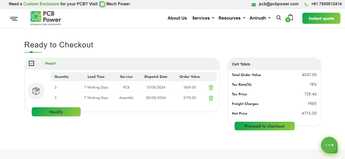 |
| ✅ | gerber.zip | |
| ✅ | schematic.pdf | Manually check schematic.pdf |
| ✅ | Source files - EasyEDA | Found both PCB and SCH files |
You can view a render of your board over on gerber.zip/2d!
Happy OnBoarding! This bot is a simpler helper for common submission types. If there's an error with this, please point it out and someone from the OnBoard team will look at it manually.
@blazecoding2009 actually I have used net labels there so all the leds are connected to the 555 , I would be really grateful if you could review the PCB once as this is my first time and I don't know wheather it's correct or not I posted it in #electronics also but no one responded there
@blazecoding2009 actually I have used net labels there so all the leds are connected to the 555 , I would be really grateful if you could review the PCB once as this is my first time and I don't know wheather it's correct or not I posted it in #electronics also but no one responded there
In the schematic, I don't see it connected to VCC/3.3v
But they are connected to the out pin(3) of the NE555P doesn't that supplies the current to it? Also please refer to the PCB also once 🙏
It does but you need a positive and negative connection to the LEDS
@LimesKey would you mind double checking for me if I'm correct here?
Looks okay in the Gerber view but the schematic is wrong like what @blazecoding2009 said. Can I ask why your LEDs are THT and so large? I think your PCB should work but some of the design decisions you did are interesting.
Also that, smd would be a better option and would look a bit better in my opinion. Tht usually Is also more pricey for PCBA
Looks okay in the Gerber view but the schematic is wrong like what @blazecoding2009 said. Can I ask why your LEDs are THT and so large? I think your PCB should work but some of the design decisions you did are interesting.
This was really my first time creating a full PCB design so I also don't know what I did but I just did it I selected THT because with the SMT I was facing issue with the bottom copper layer 🥲 Please share your thoughts and suggestions so that I could incorporate them. For the LED connection I wanted to connect all the leds one end to the out (3) so I searched how can I do it and then choice net labels, if there's something I need to change in it please let me know.
Also that, smd would be a better option and would look a bit better in my opinion. Tht usually Is also more pricey for PCBA
I was facing problem with the back layer and when I switched it worked pretty well that's why I choice it, if its possible with smt could you please share any tutorial or project with it. Then I would change it to SMT
SMD is the same as THT, just want to say that it's okay to have positive and negative on the same layer
SMD is the same as THT, just want to say that it's okay to have positive and negative on the same layer
But while creating the routes they were contradicting. I'll try once again today with SMT 👍
SMD is the same as THT, just want to say that it's okay to have positive and negative on the same layer
But while creating the routes they were contradicting. I'll try once again today with SMT 👍
Try using vias! You should seen an optoin
SMD is the same as THT, just want to say that it's okay to have positive and negative on the same layer
But while creating the routes they were contradicting. I'll try once again today with SMT 👍
Try using vias! You should seen an optoin
Thank you I'm currently a bit busy due to some assignments but I'll do it soon 👍
Hi, if you need any assistance, please don't hesitate to ask here or in #electronics on Slack. This pull request is being marked as 'Stalled' for now and will be closed in 3 days if there is no activity.
@blazecoding2009 Could you please help me out by confirming if everything is right this is my schematic so that I could move on to the pcb. Here's a 3d img also on the pcb, looking forward to your feedbacks.
What's that huge thing in the top left?
its a 1k resistor
Heres a rough pcb view
I was talking about this:
that is a resistor, that is HUGEEEE. use a smaller footprint one
I was talking about this:
that is a resistor, that is HUGEEEE. use a smaller footprint one

Done
Hey @anirudh12032008
Good luck! I've just sent your grant
Thank you could you please review the circuit once that it would be working? Please
You're good
I have uploaded all the new files and also placed the order, Thank you ♥ Should I create another PR for that?