OnBoard
 OnBoard copied to clipboard
Add "LightUp" board
Submission Checklist:
-
[x] I am a current high school, middle school, or home schooled student.
- [x] I have filled out the verification form
-
[x] I have joined the
#electronicschannel on Slack -
[x] I made this board from scratch, even if I followed a tutorial
-
[x] I have followed the directions in README.md
- [x] Created a folder under
onboard/projects - [x] Filled out
TEMPLATE.mdasREADME.mdinside your project folder - [x] Uploaded
gerber.zipandschematic.pdfinside your project folder - [x] Created a folder called
srcand uploaded design files - [x] Uploaded screenshot of PCB order called
cart.pngwith all costs included - [x] I am ordering the smallest batch size (ie. JLCPCB's smallest order is for 5 boards)
- [x] If outside the US I've checked that I can afford the customs charges in my country (which isn't covered by the grant)
- [x] Created a folder under
-
[ ] (Optional) This project is from a tutorial[^1].
-
[ ] (Optional) I'm in a FIRST (FRC, FTC, FLL, etc.) team. The number is: ____
[^1]: Projects from a tutorial are 100% fine! We just want to ask so we can count how people are using tutorials.
Hi, I'm Orpheus Leap! Here to help you review your PR.
projects/LightUp:
Required files
| ✅ | README.md | A description of your project |
| ✅ | cart.png | 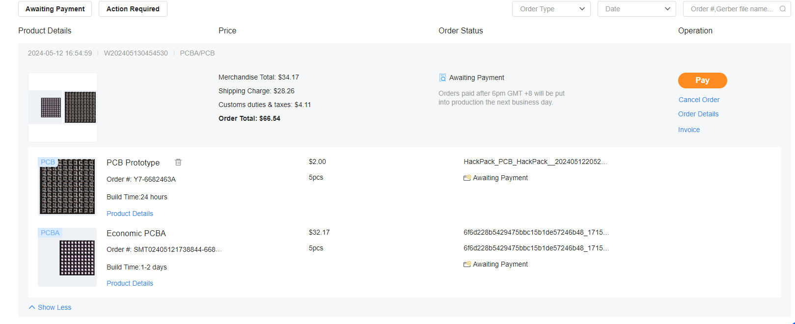 |
| ✅ | gerber.zip | |
| ✅ | schematic.pdf | Manually check schematic.pdf |
| ✅ | Source files - EasyEDA | Found both PCB and SCH files |
You can view a render of your board over on gerber.zip/2d!
Happy OnBoarding! This bot is a simpler helper for common submission types. If there's an error with this, please point it out and someone from the OnBoard team will look at it manually.
Hey @Dongathan-Jong! You can replace your WS2812's with XL-5050RGBC-WS2812B's. I've used them in several projects and they behave the same but are much cheaper and support economic assembly.
Another thing I would suggest is that if you break out your final DOUT pin, you could daisy chain multiple of these boards together
For the PCB layout, you have to make copper wires between each of the pads. The schematic connections are just theoretical, whereas your PCB layout is where the wires will actually be placed!
Also the holes for your through hole pin connector are interfering with your LEDs, you might want to move it somewhere else (and on the top layer for single sided assembly)
Hey! Thank you for the feedback :) I just changed it, could you have another look? Thanks.
You still have to connect the positive and negative traces of every other LED to the positive and negative lines. Also, the DOUT of your first LED needs to go to the DIN of the next, and so on and so forth
Basically every green wire in your schematic should have a corresponding wire in the PCB
Also, you should probably make the power traces 3-4 times thicker, because you have so many LEDs they will draw a lot of current
Your easyeda file looks perfect to me! But it looks like you might've uploaded the wrong gerber.zip and cart.png, as soon as you fix that I can get you your grant!
Hi @Dongathan-Jong! I've just sent you your grant for OnBoard. You should have received an invite in your email. There will be instructions on how to use your debit card attached should you need them. Please remember to upload your receipts when you make purchases.
Also, unfortunately, we're unable to offer support with reimbursements for customs fees, including reimbursements using leftover grant funds. Please keep this in mind before you make any purchases. More info in the OnBoard community shipping doc.
I'm looking forward to seeing your PCB be manufactured! Send pictures in the #electronics channel on Slack once you get it! Please don't hesitate to reach out if you have any questions!