Unable to Implement Ethernet UDP Protocol on SP605 Evaluation Kit (Xilinx Spartan 6 XC6SLX45t-3FGG484).
Hi (@alexforencich ),
I am trying to implement Example Design Code for Digilent Atlys (Xilinx Spartan 6 XC6SLX45) on SP605 Evaluation Kit (Xilinx Spartan 6 XC6SLX45t).
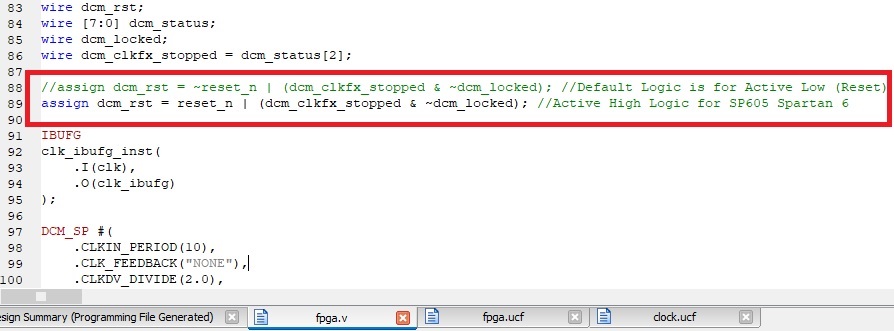
Atlys board has an Active Low Push button while SP605 has Active High. I simply invert the Logic for Reset Push Button in fpga.V as shown in the attachment. I didn't define Toggle Switches and Push Buttons in UCF (as they are not used in the code,). I then programmed SP605 and tried the ping command, but it didn't work. I'm also sending UDP data from the "Packet Sender" software, but I failed again.
I would be grateful if you could help me with some solution for SP605.
@wSafwan In line 8 of the sp605 UCF file, you've set the TIMESPEC for the sys_clk_pin to be 100000kHz, but I believe the clock input is 200 MHz. In that case the value should be 200000kHz.
Similarly, in the attached JPG I see in line 98 a value of 10 for CLKIN_PERIOD. If this refers to the sys_clk_pin then the value should be 5 instead of 10.
Hi @MJoergen , @alexforencich
These are the changes I have made so far in my project (as shown in the attached .jpg files). Although, ethernet hardware is negotiating protocols, but is unable to send and receive packets ( shows speed "1Gbps" with "no internet access" in Network Settings). Again, I tried the ping command and sent udp data from the "Packet Sender" software and monitored it through the "wireshark" software, but failed again (shows "ARP,,,, who has 192.168.1.128" in wireshark).
I’m eager to receive your feedback.
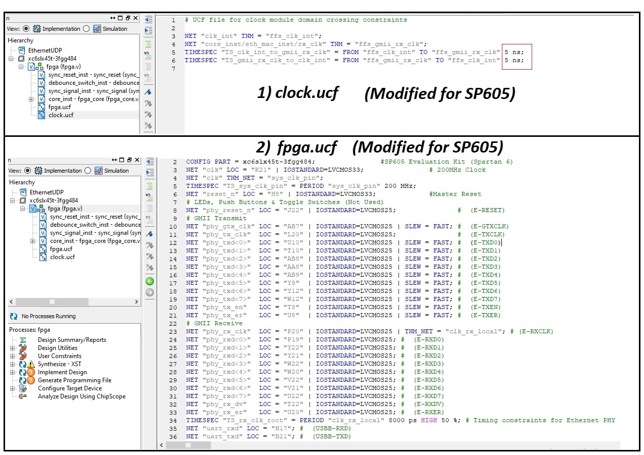
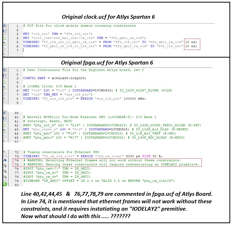
Regarding the comment on lines 74-75 I have no idea about. That must be for @alexforencich to answer.
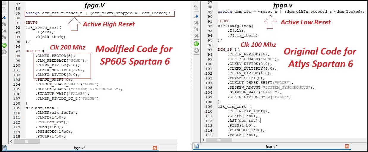
However, your fpga.v file looks wrong. As far as I understand, the input clock to the FPGA is changed from 100 MHz to 200 MHz. However, the clock output must be the same in both cases. Therefore, you should read https://www.xilinx.com/support/documentation/user_guides/ug382.pdf particularly around page 71.
The value for CLKDV_DIVIDE should probably be 4, and the value for CLKFX_DIVIDE should probably be unchanged, i.e. 2.0.
You should check in the timing report, that the DCM generates the desired frequencies.
Hmm. Agreed that something is funny about the DCM configuration, but I'm not sure offhand what the correct configuration is. It has been a very long time since I have done anything with spartan 6. As far as I can tell, CLKDV_DIVIDE only affects CLKDV, which is not used here. Only the CLKFX output is used, so only the CLKFX_MULTIPLY and CLKFX_DIVIDE values are relevant. But according to the datasheet, both of these must be integers. You could possibly try 5 and 8, but I cannot tell if this is within the operating range of the DCM. Another possibility could be to use 5 and 4 just like the ATLYS design, but set CLKIN_DIVIDE_BY_2 to "TRUE".
Hi @alexforencich , Finally, I was successful in capturing packets (along with the echo response) in wire shark. Now I want to write/store this packet to external flash memory (i.e. compact flash on SP605).
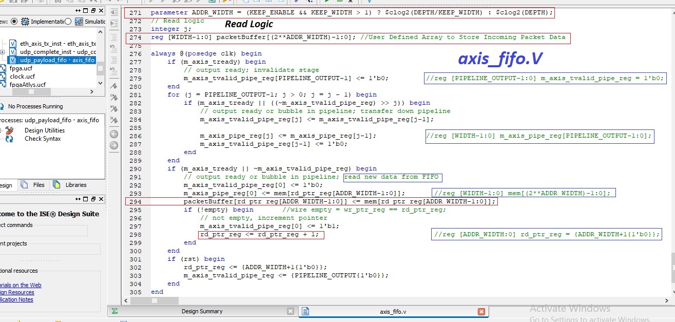
Before writing data to external flash, I did few additions in axis_fifo.V. I defined an array " reg [WIDTH-1:0] packetBuffer[(2ADDR_WIDTH)-1:0] " to store incoming packet from Ethernet Ram (i.e. " reg [WIDTH-1:0] mem[(2ADDR_WIDTH)-1:0] "). To store data byte by byte in the "packetBuffer" array, I used the instruction " packetBuffer[rd_ptr_reg[ADDR_WIDTH-1:0]] <= mem[rd_ptr_reg[ADDR_WIDTH-1:0]] " as shown in the attachment, Line 294. Now my questions are
a) Is this the correct way to store data from Ethernet RAM (mem[]) to a user defined array (i.e packetBuffer[]) as shown in Line 294 (attached attachment)? b) Which parameter is holding the input packet length (i.e. number of bytes)? c) Does the read pointer value "i.e. rd_ptr_reg" go from 0 to (packetLength-1) to store byte by byte of incoming packet after each new packet received?
I used to work on microcontroller in which I use following instructions to store data from ethernet ram. for(int i=0; i<packetLength; i++) { packetBuffer[i] = mem[i]; }
I’m eager to receive your feedback.
Well now, accessing a CF card is a whole different ball game. For that, I would probably recommend looking to some sort of a soft core to handle the CF card, since presumably you'll want a filesystem of some sort on there, and it's much easier to handle that sort of thing from a soft core. I have never poked at a CF card before from an FPGA, so I'm not going to be able to help you much with that. But, depending on the speed of the soft core and the CF card, you may want to buffer packets in DRAM before transferring them to the card, so it might make sense to bring up one of the DDR memory interfaces and use a DMA engine to transfer the packet data into DRAM, and potentially also to read the data out of DRAM to send it to the CF card. All of this is going to be significantly more complex than the UDP/IP stack in this repo.
@alexforencich Is the soft core same as IP core? is it possible and easier to send data from FPGA to PC via UART and log them on PC at a speed upto 5Mbps?
Soft core as in a soft CPU core, like microblaze or vexriscv or something. 5 Mbps is possibly a bit much for a UART. What, exactly, do you need to log?
Another thing to consider: there is an SFP slot on that board, perhaps you can use one of those SFP to base-T converter modules to get a second network port, and then send data to a PC on that second port for logging.
Hi @alexforencich Could I use "verilog-uart" ip core in integration with "verilog-ethernet" ip core (developed by you) to log data on PC by sending UDP data from the "Packet Sender" software to FPGA?